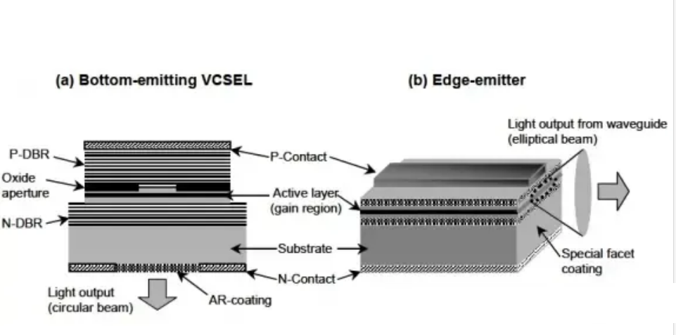
The basic structure of VCSEL includes from top to bottom: P-type ohmic contact electrode, P-type doped DBR, oxide confinement layer, multi-quantum well active region, N-type doped DBR, substrate and N-type ohmic contact electrode. Here is a cross-sectional view of the VCSEL structure [1]. The active area of the VCSEL is sandwiched between the DBR mirrors on both sides, which together form a Fabry-Perot resonant cavity. The optical feedback is provided by the DBRs on both sides. Usually, The reflectivity of DBR is close to 100%, while the reflectivity of upper DBR is relatively lower. During operation, current is injected through the oxide layer above the active area through the electrodes on both sides, which will form stimulated radiation in the active area to achieve laser output. The output direction of the laser is perpendicular to the surface of the active area, passes through the surface of the confinement layer, and is emitted from the low-reflectivity DBR mirror.

After understanding the basic structure, it is easy to understand what the so-called "vertical emission" and "parallel emission" mean respectively. The following figure shows the light emission methods of VCSEL and EEL respectively [4]. The VCSEL shown in the figure is a bottom-emitting mode, and there are also top-emitting modes.

For semiconductor lasers, in order to inject electrons into the active area, the active area is usually placed in a PN junction, electrons are injected into the active area through the N layer, and holes are injected into the active area through the P layer. In order to obtain high lasing efficiency, the active region is generally not doped. However, there are background impurities in the semiconductor chip during the growth process, and the active region is not an ideal intrinsic semiconductor. When the injected carriers combine with impurities, the lifetime of the carriers will be reduced, resulting in a reduction in the lasing efficiency of the laser, but at the same time it will increase the modulation rate of the laser, so sometimes the active region is intentionally doped. Increase the modulation rate while ensuring performance.
In addition, we can see from the previous introduction of DBR that the effective cavity length of VCSEL is the thickness of the active area plus the penetration depth of DBR on both sides. The active area of VCSEL is thin, and the overall length of the resonant cavity is usually several microns. EEL uses edge emission, and the cavity length is generally several hundred microns. Therefore, VCSEL has a shorter cavity length, a larger distance between longitudinal modes, and better single longitudinal mode characteristics. In addition, the volume of the active area of VCSEL is also smaller (0.07 cubic microns, while EEL is generally 60 cubic microns), so the threshold current of VCSEL is also lower. However, reducing the volume of the active area shrinks the resonant cavity, which will increase the loss and increase the electron density required for oscillation. It is necessary to increase the reflectivity of the resonant cavity, so VCSEL needs to prepare a DBR with high reflectivity. . However, there is an optimal reflectivity for maximum light output, which does not mean that the higher the reflectivity, the better. How to reduce light loss and prepare high-reflectivity mirrors has always been a technical difficulty.


